
Wafer Cleaning Equipment Market Size to Hit $15.61 Billion by 2033 | Research by SNS Insider
Wafer Cleaning Equipment Market Growth is driven by advanced node scaling, rising semiconductor fabrication, demand for defect-free wafers, and adoption of single-wafer, eco-efficient, and automation-driven cleaning technologies.
Austin, Dec. 14, 2025 (GLOBE NEWSWIRE) -- Wafer Cleaning Equipment Market Size & Growth Insights:
According to the SNS Insider,“The Wafer Cleaning Equipment Market size was USD 10.23 Billion in 2025E and expected reach USD 15.61 Billion by 2033, expanding at a CAGR of 5.43% during 2026-2033.”
Market Growth is Driven by the Increasing Need of Wafer Cleaning Equipment for Electronics Globally
The market for wafer cleaning equipment is expanding due to the increasing need for electronic gadgets with better performance and cleanliness. In order to ensure that the chips fulfill these requirements and offer the expected performance, wafer cleaning equipment is crucial to this process. The rise in smart devices and cutting-edge networks like 5G emphasizes how crucial premium chips are. The situation remains the same in the printed electronics industry, where a new market for advanced wafer cleaning technology has emerged.
Get a Sample Report of Wafer Cleaning Equipment Market Forecast @ https://www.snsinsider.com/sample-request/4371
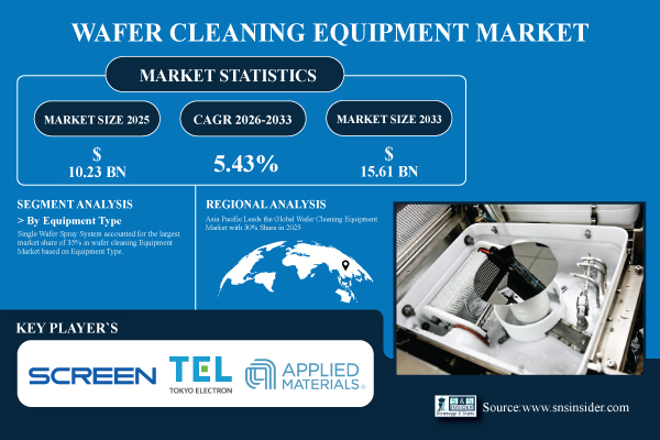
Leading Market Players with their Product Listed in this Report are:
- SCREEN Holdings Co., Ltd.
- Tokyo Electron Limited
- Lam Research
- Applied Materials
- Shibaura Mechatronics Corporation
- Akrion Technologies
- Modutek.com
- PVA TePLA AG
- Entegris
- ULTRON SYSTEMS, INC.
- Veeco Instruments Inc .
- SEMES
- AXUS Technology
- Beijing TSD Semiconductor Equipment Co., Ltd.
- Toho Kasei Co., Ltd.
- Cleaning Technologies Group
- SEMETEK
- AP&S International GmbH
- ITW
- RENA Technologies GmbH
Wafer Cleaning Equipment Market Report Scope:
| Report Attributes | Details |
| Market Size in 2025E | USD 10.23 Billion |
| Market Size by 2033 | USD 15.61 Billion |
| CAGR | CAGR of 5.43% From 2026 to 2033 |
| Report Scope & Coverage | Market Size, Segments Analysis, Competitive Landscape, Regional Analysis, DROC & SWOT Analysis, Forecast Outlook |
| Key Segmentation | By Equipment Type(Single Wafer Spray System, Single Wafer Cryogenic System, Batch Immersion Cleaning System, Batch Spray Cleaning System and Scrubbers) By Wafer Size(Less than Equals 150 mm, 200 mm, 300 mm) By Application(MEMS, CIS, Memory, Logic, RF Devices, LED, Interposer and Others) |
Purchase Single User PDF of Wafer Cleaning Equipment Market Report (20% Discount) @ https://www.snsinsider.com/checkout/4371
Lack of Regular Maintenance Can Impede Market Growth Globally
However, the demand for wafer cleaning equipment may be constrained by environmental considerations. Dust micronization and hazardous waste are produced by this activity. These contaminants are extremely dangerous to both the environment and human health if improperly managed. The optimum disposal methods for these materials are determined by strict environmental standards. For instance, powerful chemicals and rough materials may be used in the cleaning procedure. These materials must be handled and stored carefully because they are extremely hazardous or corrosive, unless mishaps would seriously contaminate the environment.
Key Industry Segmentation
By Equipment Type
The Single Wafer Spray System dominates the wafer cleaning equipment market with a 35% share as it offers unmatched precision in cleaning delicate submicron transistors. Growing demand for high-performance, miniaturized semiconductors is driving market adoption.
By Application
MEMS are set to capture a 30% revenue share in the wafer cleaning equipment market by 2025. These micro-electro-mechanical systems power critical functions in smartphones, automotive sensors, and IoT devices, where even a tiny particle can cause failure. The growth is also driven by the rising adoption of MEMS in consumer electronics and automotive applications is driving demand for advanced, highly accurate cleaning solutions.
Regional Insights:
Due to the concentration of sophisticated semiconductor factories in China, Taiwan, South Korea, and Japan, Asia Pacific is expected to hold a 30% market share in 2025, leading the wafer cleaning equipment industry. The demand for precision cleaning solutions is rising due to the rapid expansion of wearables, smartphones, electronics, and smart displays.
By 2025, the wafer cleaning equipment market is expected to develop at the fastest rate of 25% in North America due to rising investments in new semiconductor factories, growing demand for sophisticated chips made possible by AI and 5G, and government assistance from programs, such as the U.S. CHIPS Act. The demand for accurate cleaning solutions in high-performance fabs and the growth of domestic chip fabrication are the main factors driving the region's market progress.
Do you have any specific queries or need any customized research on Wafer Cleaning Equipment Market? Schedule a Call with Our Analyst Team @ https://www.snsinsider.com/request-analyst/4371
Recent Developments:
- In November 2024, SCREEN Semiconductor Solutions launched the SS-3200 for 200mm wafers, offering high-throughput spin scrubber cleaning optimized for power devices. The system reduces DI water usage and supports environmentally friendly wafer processing.
- In August 2024, Entegris signed a long term supply agreement with onsemi to provide co optimized CMP (Chemical Mechanical Planarization) solutions for SiC wafers, supporting onsemi’s silicon carbide power device manufacturing.
Exclusive Sections of the Wafer Cleaning Equipment Market Report (The USPs):
- TECHNOLOGICAL ADVANCEMENT INDEX – helps you assess the pace of innovation by tracking adoption of megasonic, brush, spray, and AI-enabled defect-detection systems, along with patent activity and automated inline monitoring upgrades across fabs.
- PERFORMANCE & EFFICIENCY METRICS – helps you evaluate equipment capabilities by measuring particle removal efficiency, defectivity reduction rates, throughput (wafers/hour), and long-term reliability such as MTBF for different wafer types.
- SCALABILITY & INTEGRATION SCORE – helps you understand how well cleaning systems integrate with CMP, lithography, and etching lines, while indicating scalability for 200mm, 300mm, and emerging 450mm wafer processing environments.
- COST & OWNERSHIP STRUCTURE ANALYSIS – helps you identify total operational and investment impact through ASP benchmarks, chemical/water/energy cost breakdowns, installation expenses, and total cost of ownership across system types.
- DEMAND & APPLICATION LANDSCAPE – helps you gauge market attractiveness by mapping adoption across logic, memory, power, and MEMS segments, regional demand shifts, and growth of eco-friendly high-throughput cleaning solutions.
- GLOBAL FAB PENETRATION MATRIX – helps you determine expansion opportunities by analyzing multi-region deployment ratios, cloud-based monitoring adoption, and installation trends across North America, Europe, and Asia-Pacific semiconductor fabs.
About Us:
SNS Insider is one of the leading market research and consulting agencies that dominates the market research industry globally. Our company's aim is to give clients the knowledge they require in order to function in changing circumstances. In order to give you current, accurate market data, consumer insights, and opinions so that you can make decisions with confidence, we employ a variety of techniques, including surveys, video talks, and focus groups around the world.
CONTACT: Contact Us:
Rohan Jadhav - Principal Consultant
Phone: +1-315 636 4242 (US) | +44- 20 3290 5010 (UK)

| About us | Network | Partners |
| Fpgroup.nlinfo@analist.nlRSS feedContactIntellectual Property Photos |
Analist.nlLinksISIN
|
MorningstarPrudena.comAAII.comNASDAQvwd GroupEuronextBATS Chi-x
|